Switched-mode power supplies (SMPS), in their various forms, are today’s go-to devices for converting AC to DC, or for converting DC at one level to DC at one or more new levels. Classical linear power supplies rectify mains AC and employ large capacitors and inductors to filter the 60-cycle pulses. SMPS’s first switch the input power on and off many thousands, or perhaps even millions, of times per second. The resulting high-frequency pulses require much lower-valued inductors and capacitors, saving precious space and improving overall efficiency.
Buck Converter Topology
The buck converter is used when a higher DC voltage has to be converted to a lower DC value. It’s often used to replace the highly inefficient linear regulator, and modern devices are 95 percent efficient or better.
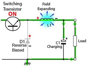
Figure 1: Buck converter, with switch turned on. (Source: Learnabout Electronics)
The diagram above is a highly simplified diagram of a buck converter. When the “switch,” usually a power MOSFET, is turned on, voltage in the inductor (L1) is generated that opposes the voltage from the source. Thus, voltage across the load and capacitor (C1) never gets as high as the input voltage from the source.

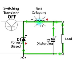
Figure 2: Buck converter, with switch turned off. (Source: Learnabout Electronics)
When the switch turns off, the energy still left in the inductor’s coil induces a voltage in the opposite direction—the same direction as initially supplied by the source. That voltage, always less than the source’s, passes through the load and the capacitor, and the diode turns on, replacing the now-disconnected power source to complete the loop.
Thus, the voltage across the load is always less than that of the voltage source. The capacitor stores power, and as the power stored in the inductor’s magnetic field begins to wane, the capacitor’s charge will keep current flowing into the load. The MOSFET switches on and off continuously, repeating the cycle. By choosing the correct values of inductor and capacitor, and by providing for the automatic adjustment of the times, within one on/off period, that the switch is closed or open or closed (the duty cycle), remarkable stability and efficiency is achieved.
Boost Converter Topology
The boost converter is a DC-to-DC converter that is usually used to boost the source voltage, but it can be adjusted to supply a lower voltage, too.
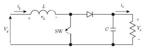
Figure 3: Boost converter. (Source: The University of Newcastle)
When the MOSFET switch is turned on, the source current builds up a magnetic field in the inductor that opposes it. When the switch is turned off, as before, the voltage switches direction. Now the source voltage, plus the voltage generated by the inductor combine to become more than the source alone. The resulting higher voltage travels through the diode, supplying Vo to charge the capacitor and flowing through the load resistance.
Then, when the switch turns on, the charge stored in the capacitor can’t flow through the diode, because the nature of the diode is to pass voltage only one way, so it stays connected only to the load resistance. As before, charge builds up in the inductor, and the cycle repeats itself.
Flyback Converter Topology
This type of switcher can operate from AC or DC voltage. Because the source power is switched on and off by the switching MOSFET directly to a transformer, this type of supply has the advantage of providing isolation between the output voltage as well as the ground and the power main. This is vitally important in many applications (see Medical Power Supplies Provide Multiple Levels of Protection).
While the detailed design of flybacks is, as in the case of all SMPS’s, quite involved, the basic principles are quite simple.

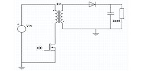
Figure 4: Flyback converter. (Source: Texas Instruments)
When the switch, generally a power MOSFET, turns on, the transformer is energized. The relationship of the transformer’s input voltage to its output voltage is determined by its windings ratio. The “dots” on the wirings of the transformer indicate that a positive voltage on the input wiring means a negative voltage will appear on the secondary. Thus, the diode will be reverse-biased, so no current flows, but a magnetic field is created in the primary (input) coil’s windings.
When the switch is turned off, the magnetic field stored in the primary induces an opposite voltage in the secondary. The diode, now forward-biased, allows the power to flow through the load and the capacitor. When the switch again turns on, the capacitor’s stored charge will only be able to discharge through the load, because the diode is, again, reverse-biased. As in the case of the previously described SMTP’s, the cycle repeats itself, and through proper choices of the transformer and the capacitor, as well as dynamic monitoring of the duty cycle, the desired output can be maintained in real-world conditions.
The Most Common Power Converter Topologies
The three topologies described in this article are perhaps the most common topologies in service today, but there are many other variations. The designer will find much of the control circuitry alluded to in the form of commercially available silicon chips, and will also find a wide choice of complete power supply units ready for use in OEM designs (see Switching Power Supplies Hit New Heights in Efficiency). In addition, research moves ahead in an effort to find ways to provide smaller and lighter power converters, and to meet the complementary goals of increased efficiency and decreased heat generation. A particularly promising topology is high-frequency resonant conversion (see Very High Frequency Resonant Conversion), which has recently made its way into commercial applications.


