Altera’s Cyclone® V SoC is an FPGA with an integrated ARM® processor that enables flexible peripheral hardware design. Its 925 MHz ARM Cortex-A9® MPCore™ processor has either a single- or dual-core option.
The ARM processor not only provides incredible performance and power efficiency, but also advanced 2D/3D graphics and signal processing acceleration through the ARM NEONTM SIMD media engine. You can easily get started designing with the Cyclone V SoC through the comprehensive documentation, strong community support, feature-rich development kits, and a wide range of design examples available.
![]()
Figure 1: Altera Cyclone V SoC Architecture
FPGAs can be intimidating for software designers. Therefore, a reliable platform, good development tools, and strong operating system support are necessary to help ease the design process. Software designers need access to system peripherals and memory bandwidth without the grief of hardware iterations. However, there is always an application-specific hardware element which must be accommodated and the challenge lies in finding a system solution that provides for both. Cyclone V SoC FPGAs are geared to meet both of these requirements with an ecosystem crafted specifically to provide the best of both worlds.
Get Started Immediately with a Development Kit
Software designers can get started immediately using an Atlas-SoC Kit, a Cyclone V SX SoC Development Kit, an Arrow Electronics SoCKit, or any other available boards, and base the underlying architecture on one of the working design examples. These boards incorporate a common set of peripheral components required in most designs, enabling immediate access to a plethora of tested and proven high-speed digital hardware that includes high-speed bus transceivers, DDR2/DDR3 memory devices, Ethernet, USB, SD card, and LCD interfacing.
Custom FPGA logic designs interface to the Cyclone V SoC hard processing system (HPS) via a standardized bus that allows simple interactions between FPGA and HPS partitions. I/O can be accessed by the GPIO application programming interface (API) and high levels of abstraction can be obtained between custom FPGA and HPS using direct memory access (DMA) memory-to-memory transfers. This is either by a HPS DMA accessed through the DMA API, or by an intelligent FPGA module with its own built-in DMA or a DMA module instantiated in Altera’s QSYS system integration tool design.
![]()
Figure 2: Atlas SOC KitF
The Atlas-SoC Kit provides an added advantage by integrating an Arduino interface header, immediately opening the doorway to a massive array of expansion boards called shields. Shields provide a drop-in prototype capability for various peripherals, including sensors, motor and servo controllers, 802.11b/g WiFi, Bluetooth, and GPS. Conversion shields are available where voltage levels are incompatible.
![]()
The Arrow SoC Kit and Cyclone V SX SoC Development Kit incorporate high-speed mezzanine card (HSMC) interfaces, enabling the use of many high-performance daughter cards, including image sensors, high-speed analog-to-digital converters, and SDI PHY interfaces.
![]()
Figure 4: Cyclone V SX SoC Development Kit and Arrow SoC Kit
Design Tools for Streamlining Designs
Hardware image compilation can be entirely makefile-driven, with an example hosted on GitHub. Altera’s SoC Embedded Design Suite (EDS) is a complete development environment, and is well documented in the Altera SoC Embedded Design Suite User Guide. The SoC EDS leverages the capability of the ARM Development Studio 5 (DS-5TM) Altera Edition Toolkit and expedites code development using a variety of utility programs and predefined run-time software with Linux application examples. A free version of the complete toolchain is also available for download.
OpenCL is becoming an increasingly popular standard for programming heterogeneous parallel devices. It is the perfect standard for maintaining a higher level of abstraction while utilizing the parallel processing power of the SoC integrated media engine, dual processors, and possible FPGA acceleration. The Altera SDK for OpenCL: Cyclone V SoC Getting Started Guide helps you set up and use the Altera SDK for OpenCL. As real-time performance is critical for many embedded designs, there is a design example available for real-time code execution profiling.
Strong Operating Systems Support
The Cyclone V SoC and its associated development kits have a comprehensive operating system ecosystem support as listed below:
![]()
- Linux is the most common general-purpose operating system used on ARM-based SoCs. The Cyclone V SoC is no different, with comprehensive support offered by both Altera and a large user community. Prebuilt Linux binaries with step-by-step instructions on how to use them are readily available. If a deeper level of customization is required, the total rebuild process is documented with the Altera Yocto open source community project.
- Android is available from a number of sources including demo kits and in various versions, including Ice Cream Sandwich.
- FreeRTOS is available for the Cortex-A9 processor on the Cyclone V SoC with detailed build instructions and examples. Detailed instructions for installing Android and several sample applications demonstrating APIs including graphics and 3D animation are available.
- VxWorks BSP from Wind River is available for the Cyclone V SX SoC Development Kit.
- Threadx from Express Logics.
- eCoSPro from eCosCentric.
More than a Processor – a Processor with a Future!
The Cyclone V SoC is more than just another ARM-based SoC . Although it offers the same benefits for software development in tools, applications, operating systems, and support as non-FPGA enabled devices, where it comes into its own is in the areas of integration, acceleration, customization, and upgradability.
Integration
Most embedded applications require application-specific hardware. Many designs require dedicated microcontrollers to manage interfaces or perform signal processing to offload the operating system. Through Qsys, Cyclone V SoC designs can incorporate dedicated softcore microprocessors, such as the Nios® II processor, that can communicate with the system memory via the HPS interface. This customizable softcore microprocessor enables peripheral controllers and signal processing to be integrated without the need for any additional devices.
Acceleration
Customizable logic empowers the system with massive application-specific processing capability. It enables algorithms to be hardcoded and act as accelerators and even coprocessors for the ARM processor. Intensive operations otherwise impractical to implement on an ARM processor, such as high-speed receiver down/up conversion, modems, codecs, encoders, and decoders, can be implemented more efficiently with custom hardware than with software. FPGA logic incorporates hundreds of special-purpose digital signal processing (DSP) mathematic modules and small blocks of memory. These can be used in combination with logic elements to efficiently implement specific algorithms concurrently, with levels of performance unachievable by sequential instruction microprocessors.
Customization
Although the Cyclone V SoC HPS has a highly flexible and capable set of peripheral elements and I/O, an integrated FPGA enables a design to incorporate additional peripheral interfaces. As product requirements change, the customizable hardware can change with the software, allowing for the introduction of new features. As device I/O have greater flexibility, the same microprocessor is more likely to be reusable across multiple products.
Upgradability
Products can have their hardware design upgraded in conjunction with software updates. This enables complex hardware algorithms to be programmed to update the feature set and correct bugs. This also allows for improvements in hardware acceleration and parallel processing to be introduced into a design during its lifetime – enabling iterations to improve efficiency and performance. This offers a degree of ‘future proofing’, and enables a more aggressive delivery strategy to be adopted for complex hardware designs.
A Simple Example of Design Flow
Step One: Establish the Appropriate Prototyping Platform
Evaluate which development kit best meets your programming needs based on the peripherals and the device logic elements. If expansion boards are required, check the compatibility of the I/O including voltages. It is common for a rapid development project to quickly ‘knock up’ expansion boards that can be used with the development kit for any special peripheral requirements. While the hardware is being developed separately, the software design team can use a combination of development kits and expansion boards to prototype the bulk of the software design. With the documentation and open designs available for the kits, hardware designers can reuse appropriate elements of the design to reduce design risks.
Step Two: Agree to an FPGA System Architecture
Establish the underlying FPGA processor architecture with the hardware designer. Find a design example that closely matches the requirements and change the Qsys configuration to incorporate additional peripherals, memory, and interfaces. This is a good time to agree on protocols for hardware interfaces. The hardware designer may be able to prioritize developing this interface first, with the associated conditionally compiled test code to enable the interface to be designed and tested before the hardware design is complete.
Step Three: Modify an Appropriate Design Example
Find a design example closest to what you would like to do in the software domain. Choose a design example based on the selected operating system and introduce new things in stages. Consider providing a simple set of test software to help the hardware designer develop his side of the design as a priority. Doing so will enable a more rapid integration at a later stage. Do not jump straight onto the actual hardware once it is available, but first obtain a high degree of software stability before attempting to do so. There is nothing worse than debugging both hardware and software simultaneously.
Step Four: Make the Project
Ensure that someone is responsible for implementing a complete make for both software and hardware combined. This is frequently overlooked but is a vital part of controlling the build and revision process. It also removes the dependency on tool IDEs and their GUIs – enabling background building without manual intervention that can lead to errors in compilation.
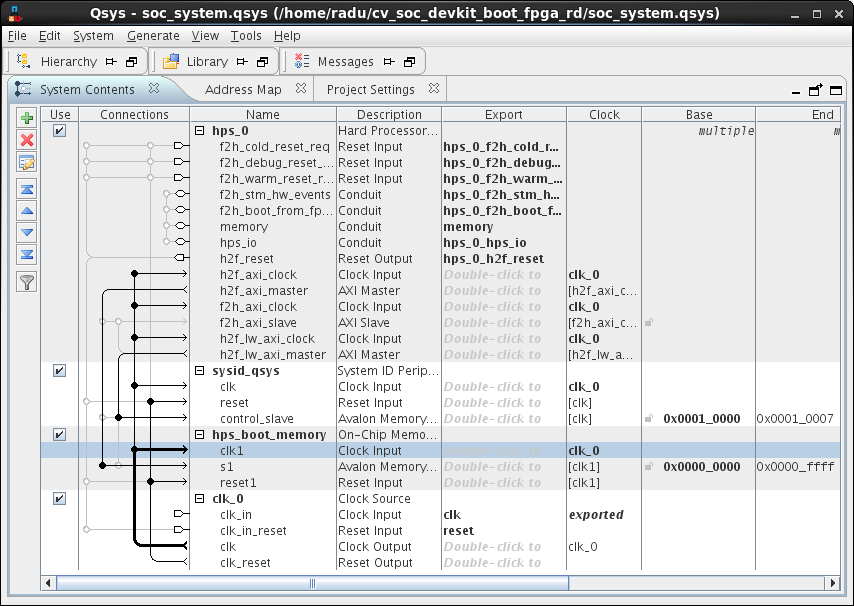
![]()
Figure 5: A System with a HPS in Qsys (View Larger)
Give it a Go!
Altera has created an SoC FPGA with both software and hardware designers in mind. This is an exciting next step in the world of increased integration and smart devices. Cyclone V SoCs blur the traditional lines between hardware and software and enable more powerful and efficient implementation, while avoiding contention between the two. Altera’s Qsys system integration tool is a fantastic tool to establish a system-level contract between software and hardware domains. The HPS-to-FPGA partitioning allows for independent development efforts with little technology understanding required between the two areas. This is a clever, exciting, and enabling technology with strong support, robust development ecosystems, and many design examples to base designs upon. Designers can start immediately by basing their architecture on one of a number of development kits and make use of the many options for expansion boards. It has never been easier to design with SoCs – Talk to an Altera representative about how they can enable the next step forward.