With the continued industry migration to things like E-commerce, remote work, and cloud computing, the demands on data centers continue to grow exponentially.
DDR4-standard DRAM has seen widespread adoption since it was adopted in 2014. However, increased customer demands for reliability, availability, and serviceability over the past few years have made it apparent that a new generation of DRAM is needed. Recently, Micron Technology, Inc announced a comprehensive Technology Enablement Program (TEP) to aid in the design, development, and qualification of next-generation computing platforms utilizing DDR5 DRAM, the most advanced currently available.
In January 2020, Micron announced its roll-out of DDR5 RDIMM samples. In July 2020, JEDEC (the global standards organization for the electronics industry) published its widely-anticipated JESD79-5 DDR5 SDRAM standard. Because of their experience with the technicalities of the new DRAM and their engagement with the new standards, companies like Micron, Cadence, Montage, Rambus, Renesas and Synopsys exist at the nexus of market demands and technical development. With the TEP, this group of businesses will work hand-in-hand with channel partners like distributors, value-added resellers, and OEMs as they develop new products using this new tech.
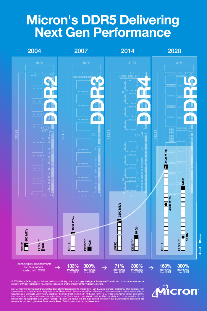
DDR5 is the most technologically advanced DRAM to date. Built off of Micron’s industry-leading 1znm process technology, DDR5 delivers an over 85% increase in memory performance. The key to this advancement is memory density - DDR5 has double that of its predecessor DDR4. In this infographic, see how DRAM has experienced exponential increases in speed over time, and how DDR5 is the best yet.

This evolution in speed allows for the increased memory bandwidth and capacity needed to power cutting-edge data centers with rapidly expanding processor core counts. The below table gives an overview of the advantages of DDR5:
| Feature/Opinion | DDR4 | DDR5 | DDR5 Advantage | |||
| Data Rates | 1600-3200 MT/s | 3200-6400 MT/s | Increases performance and bandwidth | |||
| VDD/VDDQ/VPP | 1.2/1.2/2.5 | 1.1/1.1/1.8 | Lowers power | |||
| Internal VREF | VREFDQ | VREFDQ, VREFCA, VREFCS | Improves voltage margins, reduces BOM costs | |||
| Device densities | 2Gb-16Gb | 8Gb-64Gb | Enables larger monolithic devices | |||
| Prefetch | 8n | 16n | Keeps the internal core clock low | |||
| DQ receiver equalization | CTLE | DFE | Improves opening of the received DQ data eyes inside the DRAM | |||
| Duty cycle adjustment (DCA) | None | DQS and DQ | Improves signaling on the transmitted DQ/DQS pins | |||
| Internal DQS delay monitoring |
None | DQS interval oscillator | Increases robustness against environmental changes | |||
| On-die ECC | None | 128b+8b SEC, error check and scrub | Strengthens on-chip RAS | |||
| CRC | Write | Read/Write | Strengthens system RAS by protecting read data | |||
| Bank groups (BG)/banks | 4 BG x 4 banks (x4/x8) 2 BG x 4 banks (x16) |
8 BG x 2 banks (8Gb x4/x8) 4 BG x 2 banks (8Gb x16) 8 BG x 4 banks (16-64Gb x4/x8) 4 BG x 4 banks (16-64Gb x16) |
Improves bandwidth/performance | |||
| Command/address interface | ODT, CKE, ACT, RAS, CAS, WE, A<X:0> |
CA<13:0> | Dramatically reduces the CA pin count | |||
| ODT | DQ, DQS, DM/DBI | DQ, DQS, DM, CA bus | Improves signal integrity, reduces BOM costs | |||
| Burst length | BL8 (and BL4) | BL16, BL32 (and BC8 OTF, BL32 OTF) |
Allows 64B cache line fetch with only 1 DIMM subchannel. | |||
| MIR (“mirror” pin) | None | Yes | Improves DIMM signaling | |||
| Bus inversion | Data bus inversion (DBI) | Command/address inversion (CAI) | Reduces VDDQ noise on modules | |||
| CA training, CS training | None | CA training, CS training | Improves timing margin on CA and CS pins | |||
| Write leveling training modes | Yes | Improved | Compensates for unmatched DQ-DQS path | |||
| Read training patterns | Possible with the MPR | Dedicated MRs for serial (userdefined), clock and LFSR -generated training patterns |
Makes read timing margin more robust | |||
| Mode registers | 7 x 17 bits | Up to 256 x 8 bits (LPDDR type read/write) |
Provides room to expand | |||
| PRECHARGE commands | All bank and per bank | All bank, per bank, and same bank | PREsb enables precharging-specific bank in each BG | |||
| REFRESH commands | All bank | All bank and same bank | REFsb enables refreshing of specific bank in each BG | |||
| Loopback mode | None | Yes | Enables testing of the DQ and DQS signaling |
Micron DDR5 Technical Engagement Program (TEP) Benefits:
Approved partners can get access to:
- Technical resources such as data sheets, electrical, thermal and simulation models to aid in product development and platform bring-up.
- Select DDR5 component and module samples as they become available.
- Connection with other ecosystem partners that can aid in the design and bring up of DDR5 enabled platforms.
- Technical support and training materials.

