When an application requires a voltage higher than 50V or a MOSFET of only a few milliohms, there’s no available integrated solution. Instead, you have to design a standalone MOSFET or IGBT with a gate driver.
A MOSFET is not a simple device that turns on and off instantly. It has parasitic components, shown here on Figure 1, that take on great significance when working with high power.
For instance, the lower the RDson of the MOSFET, the higher the input capacitance. A value in the thousands of pF is common.

When turning on a MOSFET, you have to charge capacitors. Depending on the size of the capacitor, different current values are used. Most families of drivers are split among these values: 500mA, 1A, 2A, and 4A. The Analog Devices, Inc. portfolio focuses mainly on 2A and 4A. To fine tune the desired current on the gate pin, a resistor is placed in series. This resistor influences the power dissipation on one side and the EMI effects on the other. Therefore a trade-off must be determined during the application design-in phase.
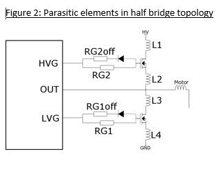
The half bridge is a common topology, but it faces two tricky issues: below ground voltage on the output pin, and the induced turn-on phenomenon. In addition to parasitic components due to the semiconductor device, the board layout brings new parasitic components, shown in Figure 2 as L1, L2, L3, and L4. A good design must limit the effects of these parasitic elements.

Induced Turn-On Phenomenon:
When a MOSFET is turned off, there is a risk that it will accidentally turn on while its companion on the same half-bridge is switching on because of Miller parasitic capacitance. The current injected on the gate by Miller parasitic capacitance causes an undesired voltage increase on the gate of the MOSFET. Induced gate voltage depends on the absolute value of the parasitic capacitance CGS, its relative ratio with CGD, the value of the dVOUT/dt of the half-bridge, and the value of the equivalent (turn-off) resistance between the source and the gate. Figure 3 illustrates this phenomenon.

To minimize this risk, there are three recommended actions:
- Reduce the resistance path between gate and source. The voltage drop on the gate is then reduced.
- Reduce the maximum Vout/dt. This reduction can be achieved by increasing the gate resistor value, which limits the gate current for the turn-on of the MOSFET. The drawback to this is the consequent increase of the switching time which means more power is dissipated during commutations.
- Use a MOSFET with a low CGD/CGS ratio.
Below Ground Voltage on the OUT pin
When the high side of the H-bridge is off, the current recirculates in the lower side (see figure 4). During the transition the diode begins to carry the entire load current for a very short period of time (a few nanoseconds). With parasitic inductances, an undershoot spike occurs. The best strategy to minimize this undershoot is to decrease the di/dt by slowing down the turn-off of the high side MOSFET. Board layout is also paramount in minimizing parasitic inductance, these two layout tips can help:
- Inductance and resistance are directly proportional to the trace’s length and inversely proportional to its width. This means it’s best to have only a small area between drivers and MOSFETs. Put both power switches for each half-bridge as close as possible to one another in order to make traces as short and wide as possible between the low-side drain and the high-side source.
- Use inductance free shunt resistors.
These implementations will usually suffice, but if the voltage spike is still considered too strong, active components like a high-voltage fast diode between the ground pin and the OUT pin will clamp the below ground voltage spike.

With these tips, you can design a standalone MOSFET or IGBT with a gate driver that can fit your specific needs.
Voir les produits connexes


